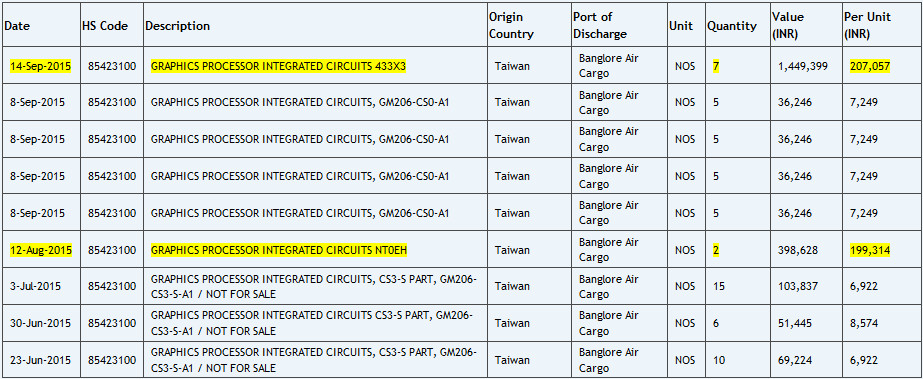
NVIDIA's next-generation flagship graphics processor, codenamed "GP100," has reportedly graduated to testing phase. That is when a limited batch of completed chips are sent from the foundry partner to NVIDIA for testing and evaluation. The chips tripped speed-traps on changeover airports, on their way to NVIDIA. 3DCenter.org predicts that the GP100, based on the company's "Pascal" GPU architecture, will feature no less than 17 billion transistors, and will be built on the 16 nm FinFET+ node at TSMC. The GP100 will feature an HBM2 memory interface. HBM2 allows you to cram up to 32 GB of memory. The flagship product based on GP100 could feature about 16 GB of memory. NVIDIA's design goal could be to squeeze out anywhere between 60-90% higher performance than the current-generation flagship GTX TITAN-X.
작성자 : 니콜라테슬라
추천 : 2
조회수 : 589회
댓글수 : 6개
등록시간 : 2015/09/22 20:19:08


 글쓰기
글쓰기